136 points by sroussey 29 days ago | 8 comments
Red_Comet_88 29 days ago
Does anyone know why Nvidia chose to re-use the 4N process for their Blackwell series? From everything I've read, 3N is mature and is already in full production, yet Nvidia chose to just reuse 4N. It seems very much unlike Nvidia to leave performance on the table.
ksec 29 days ago
N3 is mature and is already in full production for small Mobile SoC only.

The Blackwell goes up to ~750mm2 it is a completely different beast. And Nvidia is already having trouble trying to fill up their Blackwell on a higher capacity, relatively mature N4 Node. Imagine doing it on an expensive N3, and then charge $4999 only to get outrage as rip off on HN and reddit.

Generally speaking the larger die size, high performance chip tends to be a node behind simply because all the leading edge node and tools aren't even designed for them but are specifically aiming at Mobile SoC. Then you add in cost issue and yield.

wtallis 28 days ago
Surely you don't believe that large chips like Apple's M3 Max and M4 Max shipped while yields were still immature. So do you think that the wafers per month that TSMC is now cranking out over a year after N3B chips started landing in consumers hands still don't qualify as "full production"? How many fabs need to be fully devoted to 3nm before it is enough volume for you to consider it "full production"?
bigtimesink 28 days ago
The number of M3 and M4 SKUs suggests they have yield problems and are disabling bad memory and cores.
wtallis 28 days ago
"Disabling bad memory" as in DRAM isn't a thing that happens, to anybody. DRAM is made in its own fabs and goes through QA before being packaged. So whether it lands onto DIMMs or in a SoC package, it's known-good dies that are being used.

And you cannot look at the number of SKUs without also taking into account how many different die designs are being manufactured and binned to produce that product line. Intel and AMD CPUs have far more bins per die, and usually fewer different die sizes as a starting point. Apple isn't manufacturing a M3 Max and sometimes binning that down to a M3 Pro, or a M3 Pro down to a M3. You're really just seeing about two choices for enabled core count from each die, which is not any kind of red flag.

phonon 28 days ago
Memory = on chip cache. M4Max has loads of it....
wtallis 28 days ago
Disabling cache as a binning strategy isn't too common these days, unless it's a cache slice associated with a CPU or GPU core that's being disabled. Large SRAMs are manufactured usually with some spare cache lines so that they can tolerate a few defects while still operating with the nominal capacity. SRAM defects are usually not the driving force behind a binning decision.

Back when Intel was stagnant at 4 cores for the bulk of their consumer CPU product line, they did stuff like sell i7 parts with 8MB L3 cache and i5 parts with 6MB cache, more as a product segmentation strategy than to improve yields (they once infamously sold a CPU with 3MB last level cache and later offered a software update to increase it to 4MB, meaning all chips of that model had passed binning for 4MB). Nowadays Intel's cache capacities are pretty well correlated with the number of enabled cores. AMD usually doesn't vary L3 cache sizes even between parts with a different number of enabled cores: you get 32MB per 8-core chiplet, whether you have 8 cores or 6 cores enabled.

I don't know to what extent the cache sizes on Apple's chips vary between bins, but it probably follows the pattern of losing only cache that's tied to some other structure that gets disabled.

phonon 28 days ago
Yes...cores (CPU and GPU) have large caches. If the cache (or associated slice) is busted, so is the core.
nsteel 29 days ago
This. The IP they need, specifically the SerDes, isn't available for 3nm (n3e) yet. That stuff isn't required for consumer devices, it comes later.
JackYoustra 29 days ago
I'm not familiar with the process enough to even know what to search here, do you have some recommended reading materials about how IP becomes available for different processes and what the engineering difficulties / process is, especially for different types of IP?
nsteel 28 days ago
I'm sorry I don't have that. It's partly supply and demand and looking at what the early adopters (Apple, these days) need. And then there's interplay with specs and related roadmaps (i.e. nobody develops their HBM PHY IP until the spec is mature enough). HPC traditionally requires specialist memory IP (e.g. CAM) and more SRAM varieties, so that comes later. Serdes also comes later since it pushes the process limits, both analogue and digital, and also is tied into ethernet standards. You might find public marketing material from Synopsys/Cadence?
adrian_b 29 days ago
N3B is used by Intel for its Lunar Lake, Arrow Lake S and Arrow Lake H CPUs and GPUs, so it is also in full production for high-power non-small and non-mobile chips.

Of course, even if N3B is fine for desktop CPUs and for smaller GPUs, it may still have too low yields for chips of the size of the top models of NVIDIA GPUs.

nsteel 29 days ago
Anything serious is using n3e.
lexarflash8g 28 days ago
I think yields is the main reason, although I'm not an expert in that area. If its a standard deviation difference than it will increase their manufacturing costs. Nvidia got around this from Ada--> Blackwell by simply increasing TDP for their high-end cards and adding more cores. Their is no IPC/efficiency/node improvement, if I'm not mistaken, for the first time gen-to-gen.
Strom 29 days ago
The answer is probably profit margin. It's also not unusual at all for Nvidia to leave performance on the table in terms of production nodes. I mean just look at the RTX 3000 series which was made with Samsung 8LPH, categorized as a "10nm node". Even at the time, for a late 2020 launch, TSMC already had several generations which were better, in both the "7nm" an "5nm" categories.
notnullorvoid 29 days ago
US push for local manufacturing might play into that a bit since TSMC's Arizona fab only just started producing 4nm. Nvidia is planning to provide GPUs for major US datacenter expansion, so using locally produced chips should help significantly (especially if the chip tariffs end up becoming a reality).
newfocogi 29 days ago
My guess is it's related to yield and/or large die sizes making them more susceptible to defects. I expect architectural changes in the Blackwell series matter more than performance improvements from process node.
tiffanyh 29 days ago
Doesn't Apple pay for exclusive access to N, and N+1 nodes ... shutting everyone else out from using newer node sizes.
brookst 28 days ago
That’s my understanding, more or less. It’s not like Apple pays to have capacity sitting idle, they just outbid everyone else to buy (and use) 100% of capacity.
tiffanyh 28 days ago
I believe Apple also gives/pays TSMC for the capital needed to even do the R&D to shrink the nodes in the first place.
ramshanker 29 days ago
How much would the Non-Recurrent Cost associated with designing a RISC-V CPU using this 2nm? EDA Tools, Photo-Masks, One Time Chip Design Engineer Cost, Simulation/Virtual Verification and so on. I mean every thing till tape-out.
adgjlsfhk1 29 days ago
Riscv doesn't need smaller nm. It just needs someone to actually design and release a good core design. 14nm (or 4 or anything in between) is perfectly suffient to make a Riscv chip 10x faster than any Riscv that currently exist.
zozbot234 29 days ago
14nm or so is kind of a sweet spot for general purpose chip design right now, because later nodes turn out to have higher overall per-transistor cost despite the improvement in density and area. Of course this may well change over time as even finer production nodes get developed and the existing nodes then move closer to the trailing edge.
distances 29 days ago
The article linked in another comment pointed out that cost per transistor keeps falling, and it's just the fast increasing fixed costs that make it seem otherwise.

https://semianalysis.com/2022/07/24/the-dark-side-of-the-sem...

zozbot234 29 days ago
Right, but the "fast increasing fixed costs" are what really matters usually. It's not just perception.
Dylan16807 28 days ago
It depends on how big of a run you want to do.
wuschel 29 days ago
Interesting! Could you perhaps point me towards the source where I could read up on the state of the art of chip manufacturing and the implications coming from the respective manufacture processes?
zozbot234 29 days ago
Isn't that what sites like the OP are for?
mlyle 29 days ago
Of course, on the opposite side: if you have higher Fmax and lower power, you need fewer transistors to get the same characteristics for end users.
Dylan16807 28 days ago
x86 and Arm don't "need" smaller nm either, but there is always a market in speeding up general purpose CPUs.

10x is cool but when that's still catching up it's not done.

mort96 28 days ago
There are already companies making huge, expensive, high-performance chips for x86 and ARM; chips which are operating at the limit of what's physically possible. There aren't chips which do that for RISC-V to my knowledge.
Dylan16807 27 days ago
I don't see how that changes things. The end goal is the same. x86 and Arm are much further along, but that doesn't mean they "need" better lithography any more or less than RISC-V "needs" it.
wuschel 29 days ago
What do you tbink is holding RiscV core design back? Is it the IP situation?
fngjdflmdflg 29 days ago
Not a hardware person but I read in an interview with Jim Keller that ISA itself doesn't matter that much for performance.

>[Arguing about instruction sets] is a very sad story. It's not even a couple of dozen [op-codes] - 80% of core execution is only six instructions - you know, load, store, add, subtract, compare and branch. With those you have pretty much covered it. If you're writing in Perl or something, maybe call and return are more important than compare and branch. But instruction sets only matter a little bit - you can lose 10%, or 20%, [of performance] because you're missing instructions.[0]

I've cited this article a few times already (and seen others cite it) so if this is incorrect I hope someone could correct me here. (I have to assume that you also need some sort of SIMD/Vector these days, which RVA23 has anyway, but aside from that.)

I've also read that you can port CPU cores to a different ISAs pretty easily which is what PA Semi did when Apple bought them (M1 devs). So what seems to be missing is for a bunch of senior CPU developers who worked at AMD, Intel, PA Semi/Apple or ARM to just make one for RISC-V. Not sure if that is what you meant by IP here. Tenstorrent could be one such group, and they are building RISC-V CPUs, but their focus seems to be split between that and AI accelerators. China is another good candidate.

[0] https://www.anandtech.com/show/16762/an-anandtech-interview-...

topspin 29 days ago
Most of the same was said by Jim in this live interview: https://www.youtube.com/watch?v=rfFuTgnvwgs
wuschel 28 days ago
Thanks for the answer and reference!

> Not sure if that is what you meant by IP here.

By IP I meant intellectual property. I was wondering how much designs or specific hardware developments that were essential for the performance boost (or: energy efficiency of chips, compute/W) as observed with the Apple M family of designs are locked down by patents.

EncomLab 29 days ago
Keller is just a god tier hardware guy - his ability to leverage deep understanding and then explain incredibly complex issues in a few sentences is incredible. Intel shot themselves in the foot when they let him go.
AnthonyMouse 29 days ago
One of the things that could really help here is to create a license along the lines of "GPL for hardware" and then for a company like Google or Meta to release a design under it. The design wouldn't even have to be state of the art; something with performance equivalent to a ten year old x64 design would be valuable enough that people would use it for things if it was free.

But the larger value is that then people could use it as a starting point for modifications, which would in turn have to be released under the same license. Soon you have a diverse set of designs to choose from and we can start getting open hardware into common use because using any of those designs would be a cost savings over buying or designing something equivalent, but because the license requires an open design the user can then create custom firmware etc. and we might finally start to do something about the IoT security nightmare.

duskwuff 29 days ago
> a license along the lines of "GPL for hardware"

Like the CERN Open Hardware License?

https://cern-ohl.web.cern.ch/

topspin 29 days ago
The RISC-V core designs that have emerged so far don't have nearly the amount of silicon dedicated to optimizing IPC as one sees in ARM, x86 and others: predictors, sophisticated caches, complex instruction dispatch, deep pipelines, etc. That stuff isn't provided with the RISC-V core designs you get for free or license at low cost, because it's fabulously expensive to develop, tied to the ISA and core designs for which it is created, and jealously guarded through IP law.

Will RISC-V get there eventually? People like Jim Keller are building companies around that goal. However, it will likely take years, at least, for RISC-V to approach parity.

mjevans 29 days ago
Only reasons it wouldn't all boil down to, `it wouldn't matter`. E.G. If something else that does have it gets released to free as in beer levels why bother?

Unless modern civilization ends or an easier alternative is released eventually anything Open Source will get good enough.

adgjlsfhk1 28 days ago
Building a chip is really hard, and the companies that have experience all have their own architecture that they like and no reason to make a high performance design that competes with their regular chips.
selectodude 29 days ago
3nm was over a half billion. So if costs are going up at the same rate, over a billion dollars.

https://semianalysis.com/2022/07/24/the-dark-side-of-the-sem...

monocasa 29 days ago
That article refers to those charts by McKinsey as "incorrect" and instead gives a figure of $50M-$75M for 3nm.
29 days ago
ajross 29 days ago
> This paper continued TSMC’s trend over the last several years of presenting marketing papers at IEDM instead of technical papers. [...] there are no pitches in the paper, no SRAM cell size, and that graphs are all relative

Sigh. So basically we assume this is all aspirational spin and that either they haven't finalized the parameters for the process yet or they know the numbers will be disappointing already.

The era of VLSI scaling is over for sure. Hilarious that Intel's complete failure at process development happened at exactly the moment where it could do the least damage.

zozbot234 29 days ago
That's not what they're saying - they say it's been a trend over the past several years. VLSI scaling is still continuing, and the article mentions that TSMC seems to have the best numbers, though at higher per-die cost than the authors expected or found reasonable.
ajross 29 days ago
Right, that's the spin. You have to put a "seems to" on "have the best numbers" because there are no numbers. If there numbers were the "best", then they would give them. They did not. So... they probably aren't. Or there are other complexities they don't want to reveal.
zozbot234 29 days ago
> If there numbers were the "best", then they would give them. They did not. So... they probably aren't.

I'm not sure that we can say that. They may be keeping their cards close to their chest for any number of reasons. Unless they think they also had "bad" numbers in the past several years when they were doing the same thing.

WhitneyLand 29 days ago
No, that’s not how it works.

TSMC publishes industrial research, not pure science research like a university.

In this context the amount of detail they release is careful balance of PR benefit vs. competitive advantage vs. patent status vs. keeping their talent happy because good researches want their names in prestigious journals.

ajross 29 days ago
Please. "What is the fin pitch of the process you're releasing next quarter?" is hardly an IP-compromising secret. This stuff is and always has been routine disclosure in advance of technology revisions, analogous to "Our Next Software Version Will Support X and Y". You can excuse it if you insist, but it's pretty clear that we're being primed for 2nm to be at most an incremental improvement.
nsteel 29 days ago
Does the undisputed market leader need to advertise like this? There's no other gig in town. Samsung can't yield, Intel is... Yeh.
thiago_fm 29 days ago
Is there an advantage on going 2nm given the costs? Maybe somebody can clearly answer this here on HN, I love this subject!

It's interesting how the whole valuation of TSMC(and some from NVidia) are aligned by their current advantage on the 3nm process.

Intel on 18A is literally TSMC's 3nm process + backside power delivery, which means more power efficiency, performance also less heat.

It's definitely what they need to get them back into the processor game and beat everybody, maybe we will see Apple doing designs with the Intel factory before 2030?

Hope they don't fail their deadlines: summer this year to be producing 18A, and 2026 mass production.

thunderbird120 29 days ago
>Intel on 18A is literally TSMC's 3nm process + backside power delivery, which means more power efficiency, performance also less heat.

That's a pretty serious abuse of the word "literally" given that they have nothing in common except vague density figures which don't mean that much at this point.

Here's a line literally from the article

>Based on this analysis it is our belief that Intel 18A has the highest performance for a 2nm class process with TSMC in second place and Samsung in third place.

Given what we currently know about 18A, Intel's process appears to be less dense but with a higher emphasis on performance, which is in line with recent Intel history. Just looking at the density of a process won't tell you everything about it. If density were everything then Intel's 14nm++++ chips wouldn't have managed to remain competitive in raw performance for so many years against significantly denser processes. Chip makers have a bunch of parameters they have to balance when designing new nodes. This has only gotten more important as node shrinks have become more difficult. TSMC has always leaned more towards power efficiency, largely because their rise to dominance was driven by mobile focused chips. Intel's processes have always prioritized performance more as more of their products are plugged into the wall. Ideally, you want both but R&D resources are not unlimited.

zozbot234 29 days ago
The death of Dennard scaling means that power efficiency is king, because a more power efficient chip is also a chip that can keep more of its area powered up over time for any given amount of cooling - which is ultimately what matters for performance. This effect becomes even more relevant as node sizes decrease and density increases.
thunderbird120 29 days ago
If it were that simple fabs wouldn't offer a standard cell libraries in both high performance and high density varieties. TSMC continues to provide both for their 2nm process. A tradeoff between power efficiency and raw performance continues to exist.
zozbot234 29 days ago
A standard cell can be a critical performance bottleneck as part of a chip, so it makes sense to offer "high performance" cell designs that can help unblock these where appropriate. But chip cooling operates on the chip as a whole, and there you gain nothing by picking a "higher raw performance" design.
thunderbird120 29 days ago
If that were totally true you would expect to see more or less uniform ratios of HP/HD cells mixes across different product types, but that's very much not the case. Dennard scaling may be dying but it's not dead yet. You can still sacrifice efficiency to gain performance. It's not zero sum.
zozbot234 29 days ago
What product types do you have in mind exactly? Even big server chips now use a huge fraction of their area for power-sipping "efficiency core" designs that wouldn't be out of place in a mobile chip. Power is king.
monocasa 29 days ago
Those efficiency cores would put a full core from just a few years ago to shame, and data center chips have always contained a majority niche focused on throughput and perf/watt over latency. That's nearly always been focused on somewhere closer to the 45° part of the scurve than more on the top.
tarnith 29 days ago
AMD Zen5?
dannyw 29 days ago
For datacenters and especially hyperscalers, the power and cooling bill is a huge part of the TCO.

You make somewhat more power efficient chips, you get to sell it for a lot more.

Your chips are inefficient, and you won’t be able to sell to a hyperscaler even for $0.

The latter is the position Intel is quickly arriving at for DC; Epycs are much more efficient and Intel’s wildly slashing prices.

For Apple, A-series dies are pretty small, they basically prefund a large part of TSMC and almost certainly gets the lowest prices of any customer.

That said, Apple’s strict fascination with always jumping to the latest node, even when it seems premature, puzzles me from the outside.

Aperocky 29 days ago
> That said, Apple’s strict fascination with always jumping to the latest node, even when it seems premature, puzzles me from the outside.

As a user of M1, M2 and M4, that's why I've chose Apple.

I would have gladly jumped to any laptop that supports Linux with similar power and battery life and weight/build, unfortunately that computer does not exist.

Is it time to call on garmin to make a computer? They've beat apple on the watch. I have faith in them.

thijson 29 days ago
You need high chip volumes to justify the NRE cost of going to 2nm, or you're selling your chips with very high margins (ie. Nvidia).

Just saw this podcast: https://www.youtube.com/watch?v=hvQvrLjlJN8

CEO of ASML, he sees a path for the next 5-15 years for a 2 year cadence of transistor scale doubling. That's a bit slower than 18 months, which it was earlier.

loandbehold 28 days ago
Why are American fabs built in Arizona? What's so special about AZ?
josaka 28 days ago
I suspect it's, in part, because humidity is low. The fab needs to tightly control humidity and temperature. Pulling water from air is energy intensive. Facilities team in the fab I used to work in said their most energy intensive days where the most humid days.
bigtimesink 28 days ago
Humidity in Taiwan can be very high.
mort96 28 days ago
And I'm betting that combatting that humidity is a significant cost for TSMC.
sct202 28 days ago
Motorola put a bunch of their early semiconductor facilities there in the 1950s so there has been a long history of the industry there along with relevant suppliers and trained work force. Microchip Technology, Amkor, Intel, First Solar continued the trend in the 70s/80s so there's a lot of related industry built up over the decades.
muricula 28 days ago
UberFly 28 days ago
Main reasons are a stable geology and climate, access to reliable water via the salt river project that was designated for industrial use, and the historical semiconductor presence that is already in the area. The local universities also have a strong focus on tech.
manquer 28 days ago
Taiwan is a humid island on the ring of fire , is any of the environmental factors actually all that important?
SpecialistK 28 days ago
You can't choose where you're from, but you can choose where you go afterwards.
manquer 27 days ago
Arizona seems a particularly bad place to choose freely.

Fabs consume enormous quantities of water and Arizona (and the sw) are already in precarious position, and not even a semi viable theoretical option like desalination possible in the future

SpecialistK 27 days ago
There must be something Intel, TSMC, and NXP (fmr. Motorola) saw in the area to build several fabs there.
manquer 27 days ago
Talent is the reason. Same reason taiwan works very well.
inemesitaffia 27 days ago
The water is recycled
manquer 27 days ago
>water is recycled

A sweeping statement, like plastic is recycled. It is more complex than that.

It is energy intensive (and expensive) to recycle both low purity and ultra pure water (UPW) used and for some fabs it is just 40% [1] and there is no consistent globally adopted solution, most of the tech used is still evolving and not implemented everywhere.

[1] https://spectrum.ieee.org/fabs-cut-back-water-use

m00dy 29 days ago
for those who are in the industry, it's just a marketing term.
curiousObject 29 days ago
It’s marketing, but everyone is doing it. So you have got to live with it.

It’s exaggerated, but it still represents some degree of progress.

wongarsu 29 days ago
A marketing term that will have to change. For the last couple decades every new, denser process generation just took the previous number and divided it by sqrt(2). That doesn't really work beyond 2nm.

Intel invented a new number they can count down. Do we already know what naming scheme TSMC will adopt for the next generations?

28 days ago
sylware 29 days ago
So, Intel has its better "18A" process and we have no idea when they will start production at scale and where?

Weird.

high_na_euv 29 days ago
What do you mean?

Intel says that 18A will be a thing around mid of 2025, so 4-6 months from now, I think.

Then it will upgrade to HVM between Q3 and Q1 iirc

DebtDeflation 29 days ago
In late 2013 Intel said 10nm was coming in 2015.
ant6n 29 days ago
HVM?
homebrewer 29 days ago
Apparently, it's "high-volume manufacturing".
sylware 29 days ago
Where? And the scale is to supply the whole world?
adrian_b 29 days ago
The first Intel product on 18A is the "Panther Lake" CPU for laptops.

According to what Intel claims, it will be launched in H2 2025, i.e. with commercial availability either in October or in December, depending on how quickly Intel will succeed to improve the yields of the 18A process.

caycep 28 days ago
Who's running the show now that Gelsinger is out?
mort96 27 days ago
You could've just looked that up yourself on Wikipedia? David Zinsner and MJ Holthaus are interim co-CEOs
Mistletoe 29 days ago
The whole thing is incredibly frustrating to read because no one is providing any sort of data or graphs that are beyond something you would see in a commercial.

> In terms of the overreaching Power, Performance, and Area (PPA), the paper states that the process delivers a 30% power improvement or 15% performance gain and >1.15x density versus the previous 3nm node.

Since I know the nm numbers are meaningless anymore, it’s kind of an insult to the math of 3 to 2 to call these sorts of minor improvements that.

MathMonkeyMan 29 days ago
I think that this graph sums it up pretty precisely:

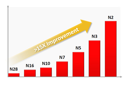
<https://semiwiki.com/wp-content/uploads/2025/02/Figure-1.jpg>

You see, the bars go up and to the right as indicated by the arrow. The thing at the top right, which is under discussion, is more than fifteen times better than the thing on the bottom left.

This is a huge achievement.

taspeotis 29 days ago
I know you’re joking but that graph is spurious:

> We took the graph image, pulled it into Excel and created an Excel graph overlaying it with the 28nm bar normalized to 1 and then entering values for the other bars until they matched the graph. If we then build a set of bars starting at 28nm = 1 scaled up based on the TSMC announced node to node power improvements we get a total improvement of less than 9x. Nodes from N28 to N10 match well but from N7 on the bars on the graph show more improvement per node than TSMC has announced. Just the N3 to N2 bars on the graph show a 55% improvements versus the announced 30% improvement.

> …

> It isn’t clear what may be driving this difference, but it is a big disconnect. This may be why the graph was removed from the final paper.

Ragnarork 29 days ago
Not sure if if this is way overblown in my head but this society, domain, and economy don't take asymptotic progress for an ok answer, and always have the pressure to deliver ever increasing performances and results, even when the law of physics become harder and harder to bend or circumvent.

It shouldn't limit innovation and trying to go past those limits one way or another, but at some point it feels like marginal (or below expectations) progress isn't acceptable at least for a while. That it then has to become coated in some marketing lie or half-truths to mask reality and oversell what it truly is... That's still progress! And it can slow down, accelerate, who knows? This should be acceptable.

29 days ago
hcfman 29 days ago
Super interesting. Now what we really need is for Raspberry Pi to make a 2nm version so that the power usage becomes more acceptable for Wildlife and biodiversity use cases.

Please, please Raspberry Pi, also make a 2nm version

Actually, I think it's broadcom I need to ask that from isn't it ?

(Although then I think it would almost become a Jetson)

Please please NVidia make a 1nm Jetson, the planet needs you to.

magicalhippo 29 days ago
The current Pi 5 is on a 16nm node[1], down from 28nm for the Pi 4.

So, far off needing a bleeding edge node[2] to see further improvements.

[1]: https://chipwise.tech/our-portfolio/raspberry-pi-5/

[2]: https://www.tsmc.com/english/dedicatedFoundry/technology/log...

Pet_Ant 29 days ago
For reference GlobalFoundries (who AMD left because they weren't willing to adopt EUV which is needed for cutting edge geometries) goes up to 12nm, so that means there is still room for Pis to improve before hitting the expensive stuff.
hcfman 29 days ago
The Pi is great! Just saying, running a Pi with an object detector on batteries draws around 9W. That's big batteries and solar or wildlife use cases. But think how cool it would be if it could run on 2W.

Having said that. The Jetson runs at around 7W doing that and a lot faster inference. Just a lot more expense. Likely the Jetson will eventually be something like 2nm. So maybe we see around 4W at that time running an object detector. And of course the Jetson has the memory and processor together on it's modules so everything can benefit. Just dropping the power on the Pi for the processor leaves that out.

But thanks for the links

magicalhippo 28 days ago
Jetson Nano was manufactured using the 20nm node as far as I can see[1].

Just goes to show manufacturing node isn't everything. There's a lot of various optimizations one can do depending on targets.

Guess we'll just have to see what the future brings.

[1]: https://en.wikipedia.org/wiki/Tegra#Tegra_X1

hcfman 28 days ago
The latest orin modules are 4nm I'm pretty sure.
my123 27 days ago
Samsung 8nm for Orin
29 days ago
rcxdude 29 days ago
The node is not nearly as relevant as the design of the SoC to optimize for low power, and the large amount of supporting software work to actually make it real. Phone SoCs are generally optimized for this, but the lifetime of a part in the market is too short for something like the raspberry pi.